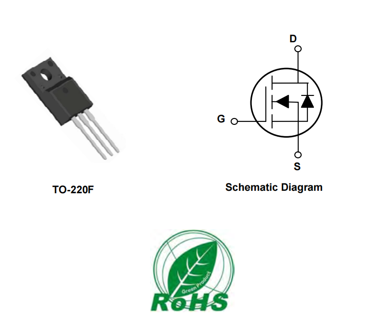
产品型号:NSU4N60
Main Product Characteristics
|
V(BR)DSS |
600V |
|
RDS(ON) |
1.9Ω(typ.) |
|
ID |
4A |
Features and Benefits
▪ Turbo HV MOSFET process technology.
▪ Low on-resistance and low gate charge.
▪ Outstanding lightning characteristics.
▪ Fast switching and reverse body recovery.
▪ High ruggedness and robustness.
The TP series products utilizes Tengxin’s turbo HV MOSFET techniques to achieve ultral low on- resistance and low gate charge. These features make this series products extremely efficient and reliable for use in power management, lighting, adapter and a wide variety of other applications.
Absolute Maximum Ratings (TC=25°C unless otherwise specified)
|
Parameter |
Symbol |
Max. |
Unit |
|
|
Drain-Source Voltage |
VDSS |
600 |
V |
|
|
Gate-Source Voltage |
VGSS |
±30 |
V |
|
|
Continuous Drain Current |
TC = 25°C |
ID |
5 |
A |
|
TC = 100°C |
3.1 |
A |
||
|
Pulsed Drain Current1 |
IDM |
20 |
A |
|
|
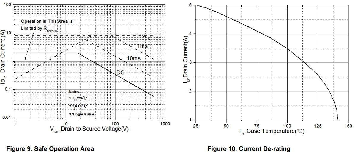
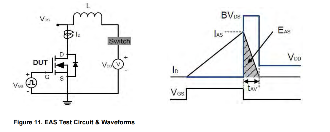
Single Pulsed Avalanche Energy2 |
EAS |
242 |
mJ |
|
|
Power Dissipation |
TC = 25°C |
PD |
40 |
W |
|
Thermal Resistance, Junction to Case |
RθJC |
3.2 |
°C/W |
|
|
Thermal Resistance, Junction to Ambient |
RθJA |
120 |
°C/W |
|
|
Operating and Storage Temperature Range |
TJ, TSTG |
-55 to +150 |
°C |
|
Electrical Characteristics (TC=25°C unless otherwise specified)
|
Parameter |
Symbol |
Test Condition |
Min. |
Typ. |
Max. |
Unit |
|
Off Characteristic |
||||||
|
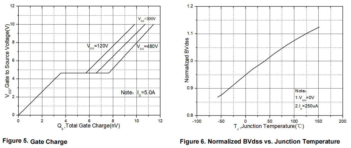
Drain-Source Breakdown Voltage |
V(BR)DSS |
VGS= 0V, ID= 250μA |
600 |
- |
- |
V |
|
Zero Gate Voltage Drain Current |
IDSS |
VDS= 600V, VGS= 0V, TJ= 25°C |
- |
- |
1 |
μA |
|
Gate to Body Leakage Current |
IGSS |
VGS= ±30V |
- |
- |
±100 |
nA |
|
On Characteristics |
||||||
|
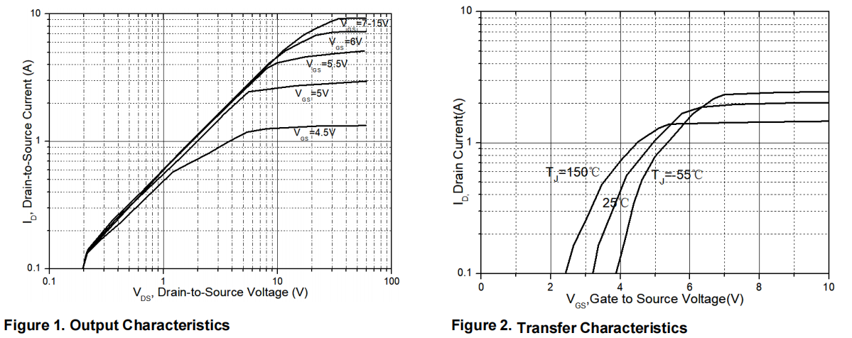
Gate Threshold Voltage |
VGS(th) |
VDS=VGS, ID= 250μA |
2 |
- |
4 |
V |
|
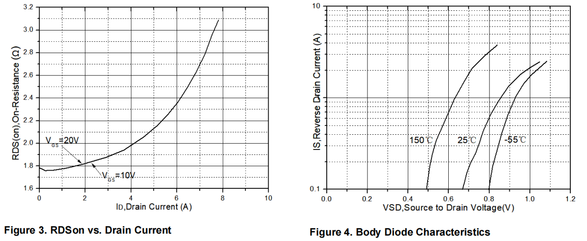
Static Drain-Source On-Resistance3 |
RDS(on) |
VGS= 10V, ID= 1A |
- |
1.9 |
2.5 |
Ω |
|
Dynamic Characteristics |
||||||
|
Input Capacitance |
Ciss |
VDS= 25V, VGS= 0V, f= 1.0MHz |
- |
479.8 |
- |
pF |
|
Output Capacitance |
Coss |
- |
62.7 |
- |
pF |
|
|
Reverse Transfer Capacitance |
Crss |
- |
2.1 |
- |
pF |
|
|
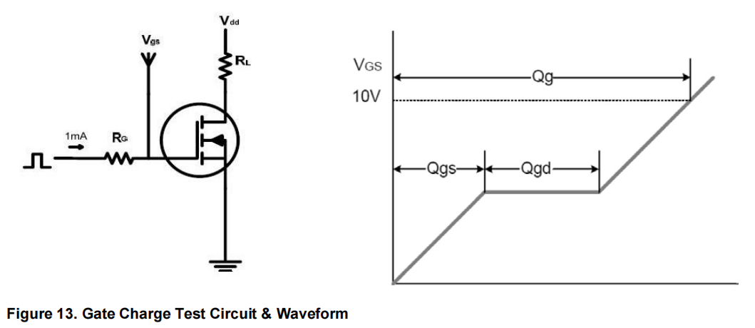
Total Gate Charge |
Qg |
VDD= 480V, ID= 2A, VGS= 10V |
- |
9.67 |
- |
nC |
|
Gate-Source Charge |
Qgs |
- |
2.74 |
- |
nC |
|
|
Gate-Drain(“Miller”) Charge |
Qgd |
- |
3.39 |
- |
nC |
|
|
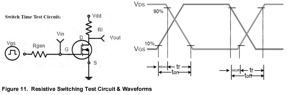
Switching Characteristics |
||||||
|
Turn-On Delay Time |
td(on) |
VDD= 300V, ID= 2A, RG= 25Ω,VGS=10V |
- |
14.8 |
- |
nS |
|
Turn-On Rise Time |
tr |
- |
28.4 |
- |
nS |
|
|
Turn-Off Delay Time |
td(off) |
- |
38.3 |
- |
nS |
|
|
Turn-Off Fall Time |
tf |
- |
21.1 |
- |
nS |
|
|
Drain-Source Diode Characteristics and Maximum Ratings |
||||||
|
Maximum Continuous Drain to Source Diode Forward Current |
IS |
|
- |
- |
5 |
A |
|
Maximum Pulsed Drain to Source Diode Forward Current |
ISM |
- |
- |
20 |
A |
|
|
Drain to Source Diode Forward Voltage |
VSD |
VGS= 0V, ISD= 2A, TJ= 25°C |
- |
- |
1.4 |
V |
|
Reverse Recovery Time |
trr |
VGS= 0V, IS= 2A, di/dt= 100A/μS |
- |
399 |
- |
nS |
|
Reverse Recovery Charge |
Qrr |
- |
2.2 |
- |
μC |
|
Notes: 1. Repetitive Rating: Pulse width limited by maximum junction temperature
2. IAS = 3.78A, L=30mH,VDD = 70V, RG = 25Ω, Starting TJ = 25°C
3. Pulse Test: Pulse width ≤ 300μS, Duty Cycle ≤ 1%

|
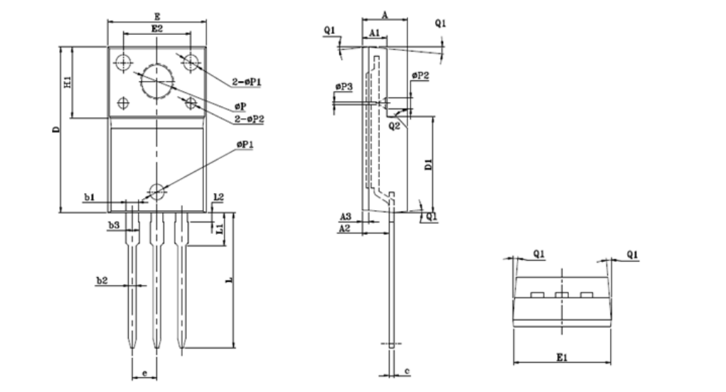
Symbol |
Dimension In Millimeters |
Dimension In Inches |
||||
|
Min |
Nom |
Max |
Min |
Nom |
Max |
|
|
E |
9.960 |
10.160 |
10.360 |
0.392 |
0.400 |
0.408 |
|
E1 |
9.840 |
10.040 |
10.240 |
0.387 |
0.395 |
0.403 |
|
E2 |
6.800 |
7.000 |
7.200 |
0.268 |
0.276 |
0.283 |
|
A |
4.600 |
4.700 |
4.800 |
0.181 |
0.185 |
0.189 |
|
A1 |
2.440 |
2.540 |
2.640 |
0.096 |
0.100 |
0.104 |
|
A2 |
2.660 |
2.760 |
2.860 |
0.105 |
0.109 |
0.113 |
|
A3 |
0.600 |
0.700 |
0.800 |
0.024 |
0.028 |
0.031 |
|
c |
- |
0.500 |
- |
- |
0.020 |
- |
|
D |
15.780 |
15.870 |
15.980 |
0.621 |
0.625 |
0.629 |
|
D1 |
8.970 |
9.170 |
9.370 |
0.353 |
0.361 |
0.369 |
|
H1 |
6.500 |
6.700 |
6.800 |
0.256 |
0.264 |
0.268 |
|
e |
2.54BSC |
0.10BSC |
||||
|
ФP |
3.080 |
3.180 |
3.280 |
0.121 |
0.125 |
0.129 |
|
ФP1 |
1.400 |
1.500 |
1.600 |
0.055 |
0.059 |
0.063 |
|
ФP2 |
0.900 |
1.000 |
1.100 |
0.035 |
0.039 |
0.043 |
|
ФP3 |
0.100 |
0.200 |
0.300 |
0.004 |
0.008 |
0.012 |
|
L |
12.780 |
12.980 |
13.180 |
0.503 |
0.511 |
0.519 |
|
L1 |
2.970 |
3.170 |
3.370 |
0.117 |
0.125 |
0.133 |
|
L2 |
0.830 |
0.930 |
1.030 |
0.033 |
0.037 |
0.041 |
|
Q1 |
3o |
5o |
7o |
3o |
5o |
7o |
|
Q2 |
43o |
45o |
47o |
43o |
45o |
47o |
|
b1 |
1.180 |
1.280 |
1.380 |
0.046 |
0.050 |
0.054 |
|
b2 |
0.760 |
0.800 |
0.840 |
0.030 |
0.031 |
0.033 |
|
b3 |
- |
- |
1.420 |
- |
- |
0.056 |