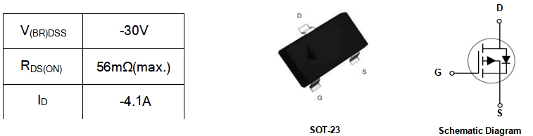
产品型号:NS3407
▪ Standard Turbo MOSFET process technology.
▪ Optimized the cell structure.
▪ Low on-resistance and low gate charge.
▪ Featuring low switching and drive losses.
▪ Fast switching and reverse body recovery.
▪ High ruggedness and robustness.

The ST series products utilizes Tengxin’s outstanding standard turbo process and packaging techniques to achieve ultral low on-resistance and low gate charge and to provide the industry’s best-in-class performance.
These features make this series products extremely efficient, temperature characteristics and reliable for use in power management, synchronous rectification, battery protection, load switch and a wide variety of other applications.
Absolute Maximum Ratings (TA=25°C unless otherwise specified)
|
Parameter |
Symbol |
Max. |
Unit |
|
Drain-Source Voltage |
VDS |
-30 |
V |
|
Gate-to-Source Voltage |
VGS |
± 20 |
V |
|
Continuous Drain Current, @ Steady-State 1 |
ID @ TA = 25°C |
-4.1 |
A |
|
Continuous Drain Current, @ Steady-State |
ID @ TA = 100°C |
-3.2 |
A |
|
Pulsed Drain Current 2 |
IDM |
-15 |
A |
|
Power Dissipation |
PD @TA = 25°C |
1.2 |
W |
|
Linear Derating Factor |
0.0096 |
W/°C |
|
|
Junction-to-Ambient (PCB Mounted, Steady-State) 3 |
RθJA |
105 |
°C/W |
|
Operating Junction and Storage Temperature Range |
TJ /TSTG |
-55 to + 150 |
°C |
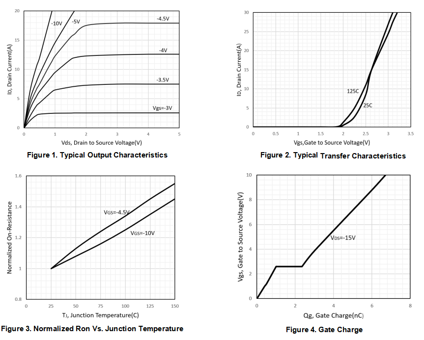
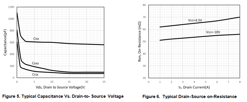
Electrical Characteristics (TA=25°C unless otherwise specified)
|
Parameter |
Symbol |
Conditions |
Min. |
Typ. |
Max. |
Unit |
|
Drain-to-Source Breakdown Voltage |
V(BR)DSS |
VGS=0V, ID=-250μA |
-30 |
- |
- |
V |
|
Drain-to-Source Leakage Current |
IDSS |
VDS=-30V, VGS=0V |
- |
- |
-1 |
μA |
|
TJ=125°C |
- |
- |
-50 |
|||
|
Gate-to-Source Forward Leakage |
IGSS |
VGS=20V |
- |
- |
100 |
nA |
|
VGS= -20V |
- |
- |
-100 |
|||
|
Static Drain-to-Source On- Resistance |
RDS (on) |
VGS=-10V, ID=-4.1A |
- |
46.5 |
56 |
mΩ |
|
VGS=-4.5V, ID=-3.5A |
- |
53 |
66 |
|||
|
Gate Resistance |
Rg |
ƒ=1MHz |
- |
4.2 |
- |
Ω |
|
Gate Threshold Voltage |
VGS (th) |
VDS=VGS, ID=-250μA |
-1.0 |
-1.6 |
-2.4 |
V |
|
Forward Transconductance |
gfs |
VDS=5V, ID=-3.0A |
- |
11 |
- |
S |
|
Input Capacitance |
Ciss |
VGS=0V VDS=-15V ƒ=1MHz |
- |
580 |
- |
pF |
|
Output Capacitance |
Coss |
- |
98 |
- |
||
|
Reverse transfer capacitance |
Crss |
- |
74 |
- |
||
|
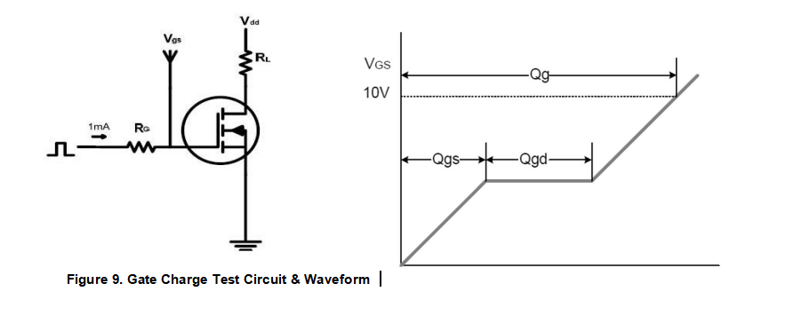
Total Gate Charge |
Qg |
ID=-4.1A, VDS=-15V, VGS=-10V |
- |
6.8 |
- |
nC |
|
Gate-to-Source Charge |
Qgs |
- |
1.0 |
- |
||
|
Gate-to-Drain("Miller") Charge |
Qgd |
- |
1.4 |
- |
||
|
Turn-on Delay Time |
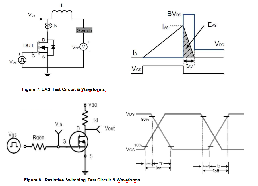
td(on) |
VGS=-10V, VDS=-15V,
ID=-1A, RGEN=2.5Ω |
- |
14 |
- |
nS |
|
Rise Time |
tr |
- |
61 |
- |
||
|
Turn-Off Delay Time |
td(off) |
- |
19 |
- |
||
|
Fall Time |
tf |
- |
10 |
- |
||
|
Source-Drain Ratings and Characteristics |
||||||
|
Parameter |
Symbol |
Conditions |
Min. |
Typ. |
Max. |
Unit |
|
Continuous Source Current (Body Diode) |
IS |
MOSFET symbol showing the integral reverse p-n junction diode. |
- |
- |
-4.1 |
A |
|
Pulsed Source Current (Body Diode) |
ISM |
- |
- |
-15 |
A |
|
|
Diode Forward Voltage |
VSD |
IS=-4.1A, VGS=0V |
- |
-0.8 |
-1.2 |
V |
Notes
1. Pulse test: Pulse Width≤300us, Duty cycle ≤2%.
2. Repetitive rating; pulse width limited by max. junction temperature.
3. Device mounted on FR-4 PCB, 1inch x 0.85inch x 0.062 inch.
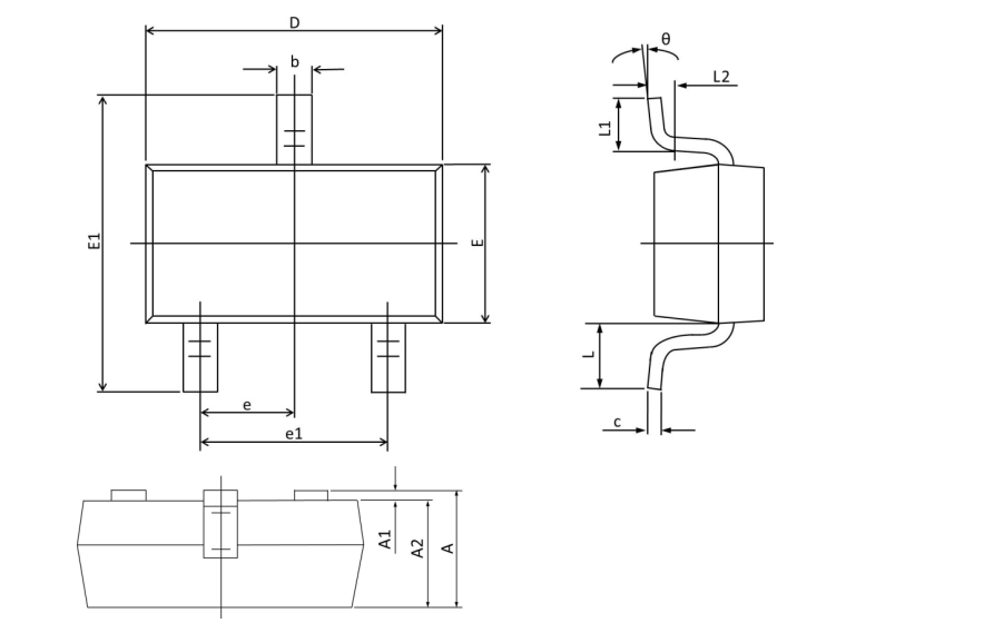
|
Symbol |
Dimensions In Millimeters |
Dimensions In Inches |
||
|
MAX |
MIN |
MAX |
MIN |
|
|
A |
1.150 |
0.900 |
0.045 |
0.035 |
|
A1 |
0.100 |
0.000 |
0.004 |
0.000 |
|
A2 |
1.050 |
0.900 |
0.041 |
0.035 |
|
b |
0.500 |
0.300 |
0.020 |
0.012 |
|
c |
0.150 |
0.080 |
0.006 |
0.003 |
|
D |
3.000 |
2.800 |
0.118 |
0.110 |
|
E |
1.400 |
1.200 |
0.055 |
0.047 |
|
E1 |
2.550 |
2.250 |
0.100 |
0.089 |
|
e |
0.95 TYP. |
0.037 TYP. |
||
|
e1 |
2.000 |
1.800 |
0.079 |
0.071 |
|
L |
0.55 REF. |
0.022 REF. |
||
|
L1 |
0.500 |
0.300 |
0.020 |
0.012 |
|
L2 |
0.25 TYP. |
0.01 TYP. |
||
|
θ |
8° |
0° |
8° |
0° |